
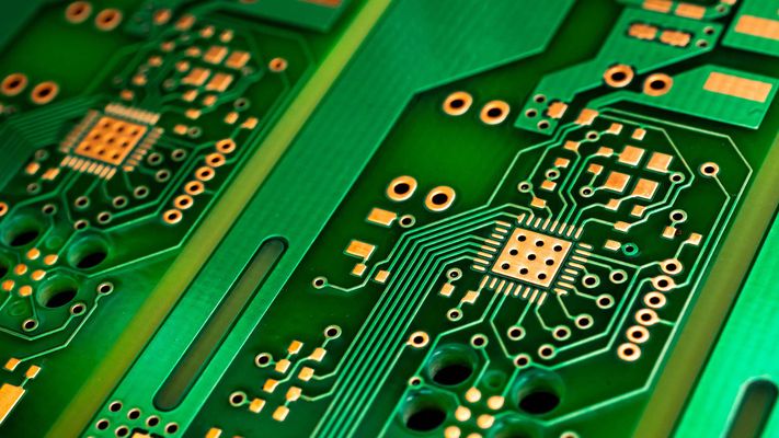
The surface finish is the last metallic coating applied to the exposed copper of a bare board before it reaches assembly. It has two jobs: keep the copper from oxidising while the board sits in storage, and present a surface that solder will wet reliably when the board finally goes through reflow. It is a small line item on a PCB quotation and one of the largest single influences on whether your solder joints turn out well.
Bare copper oxidises within hours of etching. An oxidised pad resists wetting, and a pad that does not wet properly produces a weak joint, a head-in-pillow defect, or an open circuit that passes electrical test and fails in the field. Every finish below exists to prevent that, and each one trades cost, planarity, shelf life and process compatibility differently.
How surface finishes are specified
Four of the common finishes have a dedicated IPC specification that defines the deposit and how it is measured:
| Finish | IPC specification | Current revision |
|---|---|---|
| ENIG | IPC-4552 | Rev B (2021) |
| Immersion silver | IPC-4553 | Rev A (2009) |
| Immersion tin | IPC-4554 | 2007, amended 2011 |
| ENEPIG | IPC-4556 | 2013, amended 2015 |
Two do not. HASL and OSP have no dedicated IPC final-finish specification. You will occasionally see "IPC-4555" cited for HASL; that document does not exist. An attempt to standardise OSP under that number was made in 2008 and never reached consensus. For both finishes, solderability is governed by J-STD-003, and the finish is referenced within the board specification itself (IPC-6012). If a supplier quotes you an IPC number for HASL, that is a useful signal about how carefully they read their own documentation.
A note on "Ni/Au"
"Ni/Au" is used loosely to mean ENIG, and it should not be. It describes a nickel layer under a gold layer, which covers at least four distinct finishes with very different properties and prices. ENIG is electroless nickel with an immersion gold cap, where the gold is a thin anti-oxidation layer, typically 0.04 to 0.1 µm, and solder actually wets the nickel underneath. ENEPIG adds an electroless palladium barrier between the nickel and the gold, which eliminates black pad and brings gold wire-bond capability. Electrolytic hard gold is electroplated nickel under an electroplated, cobalt- or nickel-hardened gold layer 0.4 to 2 µm thick, used as a wear surface for edge connectors and contacts, not primarily as a solder finish. Direct immersion gold (DIG) puts immersion gold straight onto copper with no nickel, a niche finish for RF and wire bonding.
Specify which one you mean. "Ni/Au" on a fabrication drawing is an invitation for the fab to choose for you.
The finishes
HASL and lead-free HASL
Hot air solder levelling floods the exposed copper with molten solder, then blows the excess off with hot air knives. It is the oldest volume finish, the cheapest, and it produces a thick, robust, genuinely long-lived solderable surface.
The surface it leaves is not flat. Solder pools in the middle of a pad and thins at the edges, and that topography is the finish's defining limitation: it is unsuitable for fine-pitch SMT, BGA and QFN packages, where an uneven pad causes bridging and inconsistent standoff.
Treat leaded and lead-free HASL as two different finishes. Leaded (SnPb) HASL is not RoHS compliant for general electronics. It survives only in out-of-scope or specifically exempted applications, and the EU has been progressively narrowing those lead exemptions. Default to lead-free HASL for anything sold into the European market, and reserve leaded HASL for exempt or legacy hardware.
Best suited to: industrial electronics, power boards, and general-purpose designs with relaxed component pitch.
ENIG (electroless nickel / immersion gold)
An electroless nickel layer, 3 to 6 µm thick, is both the solderable surface and a diffusion barrier over the copper. A very thin immersion gold cap, 0.04 to 0.1 µm per IPC-4552B, keeps the nickel from oxidising until assembly. Those numbers matter: gold thicker than about 0.1 µm buys nothing and starts to risk gold embrittlement in the joint.
ENIG is flat, corrosion-resistant, survives multiple reflow cycles, and takes aluminium wedge bonding. It is the workhorse finish for fine-pitch and high-density designs. It costs meaningfully more than HASL and it is process sensitive.
Black pad is that sensitivity made visible. During immersion gold deposition, the gold displaces nickel; if the bath is not controlled, that displacement becomes a runaway galvanic attack (hyper-corrosion) that leaves a phosphorus-rich, oxidised nickel interface. The board looks fine. The pad wets. Then the intermetallic never forms properly and the joint fractures, often after the product has shipped. The controls are phosphorus content in the 7 to 9 % band and tight management of gold bath temperature and dwell. IPC-4552B replaced the old pass/fail corrosion rule with a statistical product-rating system precisely because a single measurement was never a reliable predictor. Modern chemistries have made black pad much less common, but it remains a reason to buy ENIG from a fabricator who can show you their process data.
Best suited to: HDI, fine-pitch SMT, BGA, automotive and high-reliability assemblies.
ENEPIG
ENEPIG inserts an electroless palladium layer, 0.05 to 0.30 µm, between the nickel and the gold. The palladium stops the gold from ever reaching the nickel, which eliminates black pad outright, and it supports both aluminium wedge bonding and gold ball bonding.
It is the closest thing to a universal finish: flat, multi-reflow capable, twelve-month-plus shelf life, solderable and wire-bondable. It is also the most expensive, because it consumes both palladium and gold.
Best suited to: mixed-technology assemblies, gold wire bonding, aerospace, and automotive designs where requalification cost dwarfs the finish cost.
OSP (organic solderability preservative)
OSP is not a metal. It is an azole-based organic film, roughly 0.2 to 0.5 µm thick, that bonds to the copper and prevents oxidation until flux strips it away during reflow.
It is the cheapest finish, perfectly planar, RoHS compliant, and excellent for fine-pitch and BGA work. Its weaknesses follow from what it is: the film is consumed by flux on each thermal pass, so multi-reflow designs run out of protection after two or three cycles; there is no visual way to inspect whether the coating is intact; it cannot be wire-bonded; and it is unforgiving of handling and humidity. Bare copper under a compromised OSP film oxidises like any other bare copper.
Best suited to: single-reflow, cost-sensitive, high-density boards assembled promptly after fabrication.
Immersion tin
A chemical displacement reaction deposits a uniform tin layer directly onto the copper, at least 1.0 µm thick per IPC-4554. It is flat, lead-free, fine-pitch-friendly, and it is the best of the planar finishes for press-fit connectors.
Its limitation is often described as tin whiskering. That is the wrong mechanism to lead with. The limiting mechanism is copper-tin intermetallic growth. From the moment the tin is deposited, copper and tin interdiffuse and grow a Cu6Sn5 intermetallic layer that steadily consumes the free, solderable tin above it. That makes shelf life a hard limit rather than a soft storage guideline. It is exactly why IPC-4554 specifies a minimum deposit of 1.0 µm and only permits a reduced minimum of roughly 0.4 µm when the board will be soldered within thirty days.
Whiskers are a secondary concern, driven by the compressive stress that the same intermetallic growth creates. The classic whisker problem in the industry is associated with thicker electroplated pure tin on component leads, not with a one-micron immersion deposit on a pad. Mention it; do not build your material decision around it.
Best suited to: press-fit designs, fine-pitch SMT, and telecommunications hardware with controlled storage and short assembly lead times.
Immersion silver
A thin silver layer, 0.12 to 0.40 µm per IPC-4553A, is deposited directly on copper. It is flat, has very low contact resistance, and it is the best mainstream finish for high-frequency work.
The RF advantage is worth being concrete about. ENIG's nickel layer is magnetic and lossy; at 10 GHz it adds roughly 0.02 to 0.05 dB/cm of insertion loss compared with bare copper. Immersion silver has no nickel, so signals stay in the copper where they belong.
The cost is handling. Silver tarnishes, and in humid or sulphur-bearing environments it is vulnerable to creep corrosion and to micro-voiding at the joint interface. It needs sealed packaging, controlled storage and disciplined handling between fabrication and assembly.
Best suited to: RF and microwave circuits, high-speed digital, and any design where signal integrity dominates.
Hard (electrolytic) gold
Hard gold is electroplated nickel with a thick, hardened electroplated gold layer over it. It is a wear surface, not a solder finish. It goes on edge-connector fingers, switch contacts and anything that has to survive repeated mating cycles. It is also the finish for gold ball bonding. It is expensive, and it is normally applied selectively to the contact area rather than to the whole board.
Thickness, shelf life and process compatibility
| Finish | Deposit thickness | Typical shelf life |
|---|---|---|
| HASL (lead-free) | Uneven, tens of µm | 12 months or more |
| ENIG | Ni 3 to 6 µm, Au 0.04 to 0.1 µm | 12 months or more |
| ENEPIG | Ni 3 to 6 µm, Pd 0.05 to 0.30 µm, Au ≥ 0.03 µm | 12 months or more |
| OSP | 0.2 to 0.5 µm | 6 to 12 months |
| Immersion tin | ≥ 1.0 µm | 6 to 12 months |
| Immersion silver | 0.12 to 0.40 µm | 6 to 12 months |
Shelf life assumes the packaging and storage conditions described in IPC-1601. A board stored loose on a shelf does not get these numbers.
| Finish | Practical reflow cycles | Wire bonding | Press-fit |
|---|---|---|---|
| HASL (lead-free) | 1 | No | Yes |
| ENIG | 3 or more | Aluminium wedge only | Yes |
| ENEPIG | 3 or more | Aluminium and gold | Yes |
| OSP | 2 to 3 | No | Acceptable |
| Immersion tin | 2 | No | Yes, good |
| Immersion silver | 2 to 3 | No | Yes |
| Hard gold | Contact finish | Gold ball bonding | Yes |
Choosing a finish
Work through the constraints in this order, because the early ones eliminate options that the later ones cannot recover:
- Start with component pitch. Any board carrying fine-pitch BGA or QFN packages rules out HASL, which leaves the planar finishes.
- Check wire bonding next. Gold ball bonding means ENEPIG or hard gold, while aluminium wedge bonding also works with ENIG.
- Count the thermal passes. Double-sided reflow plus a rework cycle will exhaust an OSP film.
- Weigh signal integrity. Above a few GHz, the nickel in ENIG becomes a measurable loss term, which points to immersion silver or another nickel-free finish.
- Account for storage and assembly lead time. If boards will sit for six months before assembly, immersion tin's intermetallic clock is already running.
- Then apply RoHS scope. Use lead-free HASL unless you hold a specific exemption.
- Only now does cost enter. A finish chosen on price alone that fails one of the constraints above is the most expensive one you can buy.
For most industrial designs with mixed component sizes, lead-free HASL remains a sound, economical default. Once fine-pitch packages enter the design, ENIG is the usual answer. ENEPIG is what you specify when the qualification cost of getting it wrong exceeds the material premium.
Getting it right in procurement
Surface finish is decided during design, but it is bought as a line on a fabrication drawing. Be explicit: name the finish and its IPC specification, and state the deposit thickness you expect. "ENIG" is a request. "ENIG per IPC-4552B, nickel 3 to 6 µm, gold 0.05 to 0.10 µm" is a requirement you can inspect against.
Two related properties belong in the same conversation, because they are also bare-board characteristics that determine field reliability rather than assembly yield: the CTI value and ionic cleanliness of the board. And if you are optimising the whole fabrication package for cost, the finish interacts with the rest of the stack-up in ways covered in our design rules for low-cost PCB manufacturing.
Selecting a surface finish means balancing cost, manufacturability, assembly process and long-term reliability, and those trade-offs are cheapest to resolve in the design phase. If you would like to review a stack-up or discuss which finish suits your assembly process, our engineering team is happy to help.
Sources
- IPC-4552B, Specification for Electroless Nickel/Immersion Gold (ENIG) Plating for Printed Circuit Boards
- IPC-4553A, Specification for Immersion Silver Plating for Printed Circuit Boards
- IPC-4554, Specification for Immersion Tin Plating for Printed Circuit Boards
- IPC-4556, Specification for Electroless Nickel/Electroless Palladium/Immersion Gold (ENEPIG) Plating for Printed Circuit Boards
- J-STD-003, Solderability Tests for Printed Boards
- IPC-6012, Qualification and Performance Specification for Rigid Printed Boards
- IPC-1601, Printed Board Handling and Storage Guidelines
- EU RoHS Directive 2011/65/EU, Annex III lead exemptions