

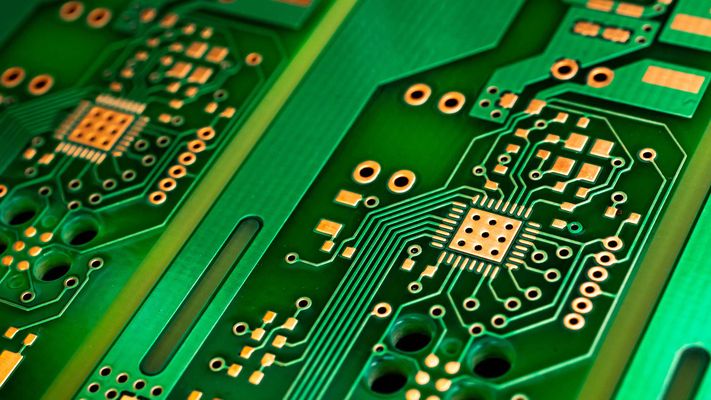
The following guideline values are intended to help manufacture printed circuit boards as cost-effectively as possible. Thus, these dimensions are not the limit of what is technically feasible, but the limit of the standard process of many PCB manufacturers. For example, holes below 150 µm can be achieved by laser drilling, but this can lead to higher unit costs and runtimes.
Trace Spacing, Annular Rings and Copper Thickness
| Copper Thickness | Trace width, annular rings and trace spacing (optimal) | Trace width, annular rings and trace spacing (minimal) |
|---|---|---|
| 18 µm | 125 µm | 100 µm |
| 35 µm | 150 µm | 100 µm |
| 70 µm | 250 µm | 200 µm |
| 105 µm | 300 µm | 250 µm |
Drill Diameters
Drilling and milling are the most cost-intensive processes in PCB production. In order to be able to manufacture at low cost, it is ideal for PCB manufacturers if PCBs can be stacked during this process. For example, 1.5 mm PCBs can ideally be milled in stacks of 3. Thinner PCBs are drilled in stacks of up to 5.
The size of the drill diameter is in proportion to the thickness of the PCB. This ratio, also called aspect ratio, should not be less than 1/10. The most favorable production can be achieved with an aspect ratio of 1/5. The following optimum and minimum smallest drill diameters result:
| PCB Thickness | Smallest Drill (optimal) | Smallest Drill (minimal) |
|---|---|---|
| 0.8 mm | 200 µm | 150 µm |
| 1.0 mm | 200 µm | 150 µm |
| 1.5 mm | 300 µm | 150 µm |
| 2.0 mm | 400 µm | 200 µm |
However, not only be careful not to choose drill diameters that are too small, but also commit to a standard diameter (e.g. 300 µm) for simple designs if possible to reduce tool changes in the drilling process and thus save costs.
Milling
It is important to minimize the milling paths on the PCB and, if possible, to use a standard milling tool of 2.4 mm. Thus, with milling tools of 1.6 to 1.2 mm, only packs of 2 can be milled, and between 1.2 and 0.8 mm, only individual PCBs can be milled. Due to wear, milling speeds and more expensive milling tools, a milling operation with a 0.8 mm milling tool costs 10 times as much as with a 2.4 mm milling tool.
PCB Panel Design
Note: Leave the PCB panel design to your electronics manufacturing firm, or speak to them about the requirements.
When designing the panels, it is important to make the best possible use of the PCB manufacturer's production dimensions. Especially in the case of multilayer PCBs, it can therefore be useful not to specify the panel size exactly, but to have it determined by the PCB manufacturer.
Typical net panel dimensions from PCB manufacturers are for example:
- 572 x 508 mm
- 567 x 427 mm
These dimensions vary significantly depending on the manufacturing equipment (exposure, plating, milling). It is very important to utilize the material as efficiently as possible.