
PCB Assembly Glossary
PCB Assembly Glossary - A-Z Manufacturing Terms - Newmatik
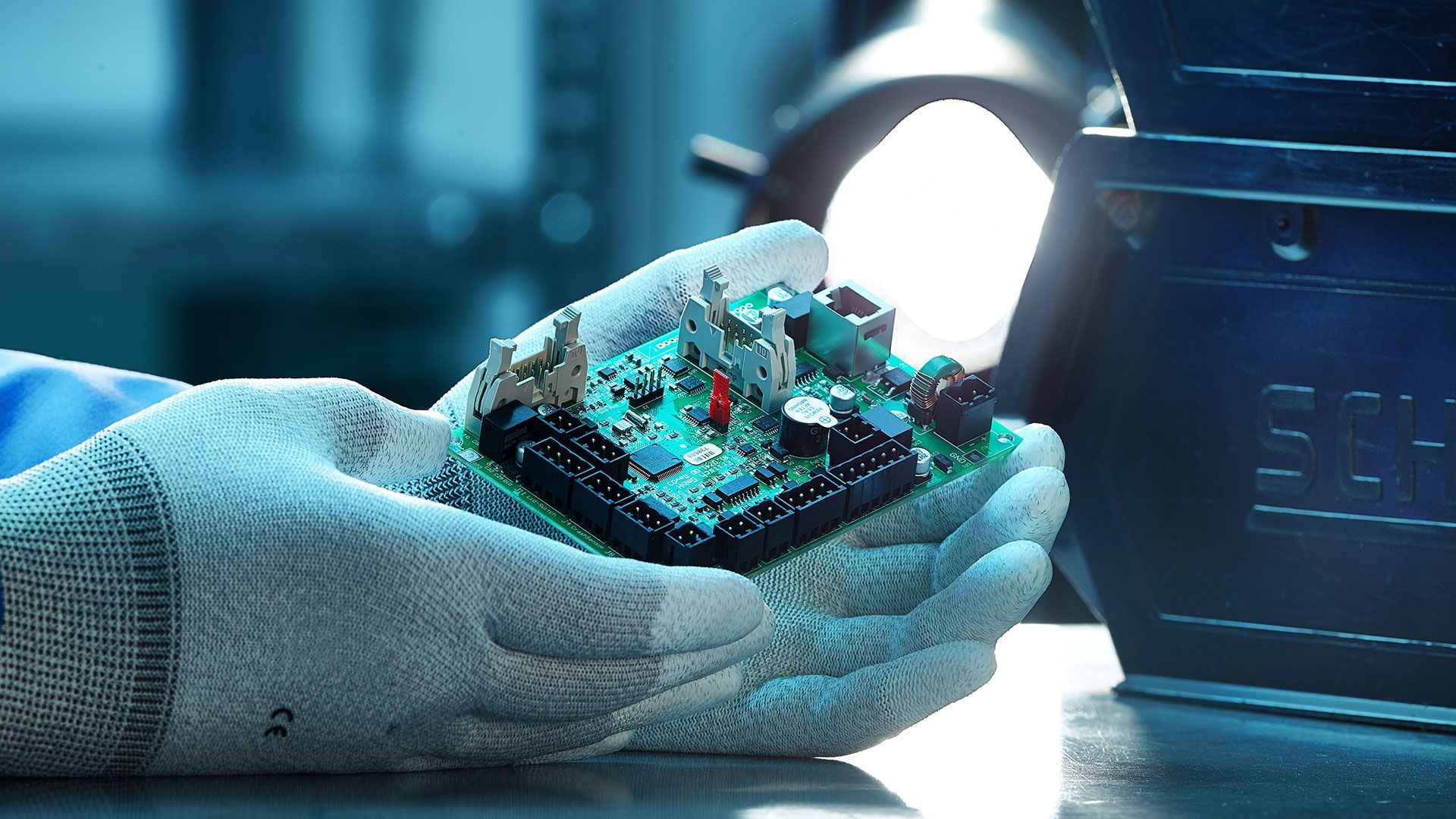
PCB Assembly Glossary - Complete A-Z Reference Guide
Comprehensive terminology guide for printed circuit board assembly, electronics manufacturing services, and PCB production. Essential reference for engineers, procurement professionals, and anyone working with PCB assembly.
A
AOI (Automated Optical Inspection): Automated camera-based inspection system that detects assembly defects. Not used at Newmatik; we use X-ray inspection and trained IPC-certified visual inspection.
Assembly Drawing: Technical document showing component placement, orientation, and reference designators for PCB assembly.
ATEX Certification: European directive for equipment used in explosive atmospheres (oil, gas, mining industries).
B
BGA (Ball Grid Array): IC package type with solder balls arranged in grid pattern on bottom. Requires X-ray inspection to verify solder joints.
Bill of Materials (BOM): Complete list of components, quantities, and specifications required for PCB assembly.
Blind Via: Via that connects outer layer to inner layer but doesn't go through entire board thickness.
Buried Via: Via connecting only inner layers, not visible from board surface.
C
CAM (Computer-Aided Manufacturing): Software process converting design files to manufacturing instructions.
Chipshooter: High-speed pick-and-place machine optimized for small passive components (0201, 0402, 0603).
Component Traceability: System tracking each component from manufacturer batch to finished assembly. Critical for medical, automotive, aerospace.
Conformal Coating: Protective polymer layer applied to assembled PCB for environmental protection.
Counterbore: Cylindrical flat-bottomed hole for recessed component mounting.
D
DFM (Design for Manufacturing): Analysis ensuring PCB design is manufacturable with acceptable yield and cost.
DNP (Do Not Place): Component shown on assembly drawing but not installed (reserved for options/variants).
DRC (Design Rule Check): Software verification that PCB design meets manufacturing constraints.
E
EMS (Electronics Manufacturing Services): Contract manufacturing of electronic assemblies. Newmatik is an express EMS provider.
ESD (Electrostatic Discharge): Static electricity discharge that can damage sensitive components. Controlled environment required.
F
FAI (First Article Inspection): Comprehensive inspection of first production unit to verify conformance to specifications.
Fiducial: Optical reference marks on PCB used by pick-and-place machines for accurate component placement.
Fine-Pitch: Components with lead spacing less than 0.65mm (often down to 0.4mm or 0.3mm).
Flux: Chemical cleaning agent used during soldering to remove oxides and improve solder flow.
G
Gerber Files: Standard file format for PCB fabrication containing layer-by-layer design data.
Ground Plane: Large copper area connected to ground potential, providing EMI shielding and low-impedance return path.
H
HASL (Hot Air Solder Leveling): PCB surface finish using solder applied by hot air to create solderable surface.
HDI (High-Density Interconnect): PCB technology with fine traces, small vias, and high connection density.
I
ICT (In-Circuit Test): Electrical test using bed-of-nails fixture to verify component presence, values, and connections.
IMS (Insulated Metal Substrate): PCB with metal core (usually aluminum) for thermal management. Common in LED and power electronics.
IPC: Association Connecting Electronics Industries. Defines quality standards (IPC-A-610, IPC-J-STD-001).
IPC Class 2: General electronic products (computers, phones). Acceptable quality level.
IPC Class 3: High-reliability electronics (medical, aerospace, military). Zero-defect tolerance. Newmatik manufactures to IPC Class 3.
J
Jet Printing: Solder paste application using inkjet-like technology. Allows rapid changeover without stencils. Used by Newmatik for express prototypes.
J-STD-001: IPC standard for soldering requirements for electronic assemblies.
K
Kapton Tape: High-temperature polyimide tape used for masking during selective soldering or wave soldering.
Keep-Out Area: PCB region where components cannot be placed (mechanical constraints, testpoint access).
L
Lead-Free: Solder alloy without lead, typically SAC (Tin-Silver-Copper). Required by RoHS directive.
Lead Time: Time from order placement to delivery. Newmatik express: 10 days or less.
M
MCM (Metal Core PCB): PCB with metal base for heat dissipation. See IMS.
Microvia: Via with diameter less than 150µm, typically laser-drilled. Used in HDI boards.
Mixed Assembly: PCB with both SMT and through-hole components.
N
NPI (New Product Introduction): Process of transitioning new design from development to production. Newmatik specializes in rapid NPI.
NRE (Non-Recurring Engineering): One-time setup costs (fixtures, programming, tooling).
O
OEM (Original Equipment Manufacturer): Company manufacturing products sold under another brand.
Odd-Form Component: Non-standard component requiring special handling (connectors, switches, displays).
P
Panelization: Grouping multiple PCBs on single production panel for efficient manufacturing.
Pick-and-Place: Robotic machine placing surface-mount components on PCB before soldering.
Pitch: Distance between component leads or pads (e.g., 0.5mm pitch BGA).
PPAP (Production Part Approval Process): Automotive industry process documenting production readiness.
PTH (Plated Through-Hole): Hole with conductive plating connecting PCB layers.
Q
QFN (Quad Flat No-Lead): IC package with pads on bottom perimeter instead of leads. Requires careful process control.
QFP (Quad Flat Package): IC package with leads on all four sides.
R
REACH: EU regulation restricting hazardous substances in products.
Reflowing: Heating process melting solder paste to create permanent solder joints in SMT assembly.
Rigid-Flex: PCB combining rigid and flexible sections. Complex assembly requiring specialized process.
RoHS: Restriction of Hazardous Substances directive limiting lead, mercury, cadmium in electronics.
S
Selective Soldering: Automated through-hole soldering of specific locations without wave soldering entire board.
Silkscreen: Text and symbols printed on PCB surface for component identification.
SMD (Surface-Mount Device): Component designed for surface mounting (vs through-hole).
SMT (Surface-Mount Technology): Assembly method placing components on board surface. Enables miniaturization and automation.
Solder Mask: Polymer coating on PCB protecting copper and preventing solder bridges.
Solder Paste: Mixture of tiny solder balls and flux applied to pads before component placement.
Stencil: Metal template for applying solder paste to specific PCB locations.
T
Testpoint: PCB location designated for electrical test probe access.
THT (Through-Hole Technology): Assembly method inserting component leads through PCB holes. Stronger mechanical connection than SMT.
Tombstoning: Defect where small component stands vertical on one end due to uneven heating.
Turnkey Assembly: Full-service PCB assembly where EMS provider procures all components and materials.
U
UL (Underwriters Laboratories): Safety certification organization. UL 94 rates PCB flammability.
V
Vacuum Vapor Phase Soldering: Soldering method using condensing vapor in vacuum. Provides void-free BGA soldering for aerospace/high-reliability applications. Available at Newmatik.
Via: Conductive connection between PCB layers.
Via-in-Pad: Via located directly in component pad, often filled/capped for flat surface.
W
Wave Soldering: Through-hole soldering method where PCB passes over molten solder wave.
Wetting: Solder flow characteristic indicating good metallurgical bond.
X
X-ray Inspection: Non-destructive inspection using X-rays to verify hidden solder joints (BGAs, QFNs). Standard inspection method at Newmatik for critical components.
Z
Zero-Defect: Quality philosophy requiring no defects in production. IPC Class 3 standard.
Related Resources
About Newmatik PCB Assembly
Newmatik provides express PCB assembly in 10 days or less with complete online ordering platform. We manufacture to IPC Class 3 standards with full component traceability, X-ray inspection, and 35 years of expertise. Made in Germany and Romania, shipped worldwide.
Keywords: PCB assembly, PCBA, electronics manufacturing, SMT assembly, express EMS, rapid prototyping, online PCB assembly, IPC standards