

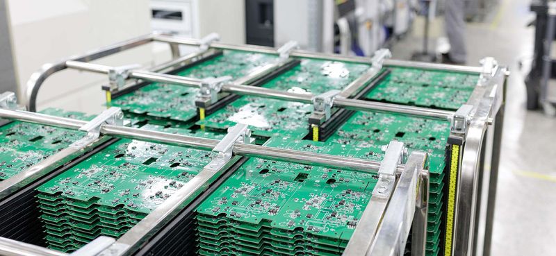
In the manufacturing of Printed Circuit Boards (PCBs), panelization involves arranging multiple PCBs on a larger panel for efficient mass production using automated SMD assembly machines. There are two primary methods to connect individual PCBs within a panel: perforated tabs and V-cuts. Our preferred method is the V-cut due to its advantages in production efficiency and product quality.
Why Panelization Is Necessary
- Cost Efficiency: Processing multiple PCBs at once reduces machine setup times and operational costs.
- Enhanced Machine Compatibility: Most PCB assembly machines are designed to handle larger panels rather than individual, smaller boards. Panelization aligns with the equipment's capabilities, enabling simultaneous fabrication and assembly of multiple PCBs, thereby maximizing throughput.
- Improved Handling and Stability: Handling individual PCBs, especially smaller sizes, can be delicate and prone to damage. Panelization stabilizes these smaller units in a larger, more robust format, making them easier to manage through various production stages such as assembly, reflow-soldering, and inspection.
- Quality and Consistency: Uniform production conditions are more easily maintained when PCBs are fabricated on a panel.
Connection Methods: Perforated Tabs vs. V-Cut
Perforated Tabs
| Aspect | Details |
|---|---|
| Description | This method involves holding the PCBs in the panel using small tabs, which are later sheared or milled to separate the individual boards. |
| Pros | Provides strong physical support and can be used to connect rounded shapes. |
| Cons | More labor-intensive to separate, might require additional finishing to smooth edges, and can lead to stress at break points, potentially damaging the PCB. |
V-Cut (Preferred Method)
| Aspect | Details |
|---|---|
| Description | A V-cut is a pre-scored line created on the panel that allows the PCBs to be easily separated. The cut, shaped like a "V," penetrates part of the way through the panel. |
| Pros | Quick and easy separation with minimal stress on the PCBs, provides a cleaner edge than perforated tabs, and reduces the need for post-processing. |
| Cons | Slightly less supportive for very heavy or thick PCBs. |
Ideal Panel Design
Follow our panel design drawing to create optimized PCB panels.
