

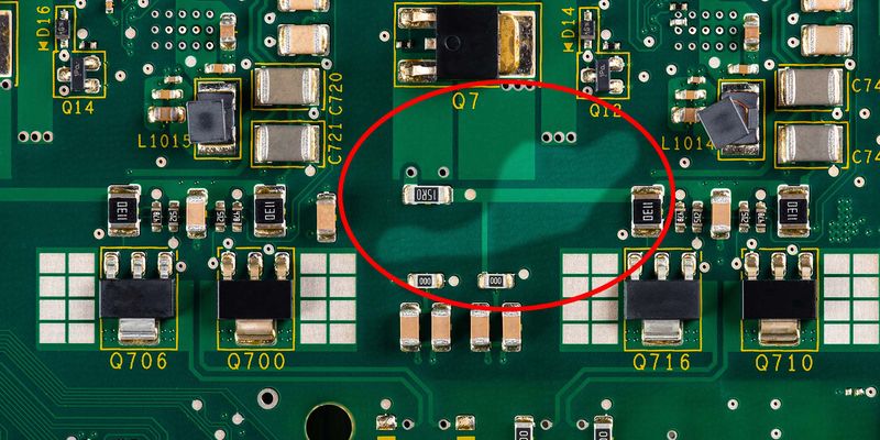
- Printed Circuit Board (PCB) delamination is the physical separation of the layers of a PCB
- It is typically observed in the laminate of the actual PCB during visual inspection
- It can also occur in the internal layers
- When delamination occurs in internal layers, it may cause malfunctions
- The cause of this malfunction will be difficult to pinpoint without thorough examination of the PCB layers
How does PCB delamination affect the final assembly?
PCB delamination affects the final assembly in two (2) ways:
- Visually - because it produces unwanted blister spots in the PCB
- Technically - because it causes interference with the internal layers of the PCB, which may cause circuit malfunctions
What causes PCB delamination?
- PCB delamination occurs because humidity gets trapped in the internal layers
- The trapped moisture fails to escape through other areas of the PCB
Moisture trapped during the PCB manufacturing process
- PCB manufacturing involves a series of "wet" processes, especially for multi-layer PCBs
- Various types of liquid and/or chemicals are used to manufacture the PCB
- During these processes, the PCB material tends to absorb moisture
- This moisture collects in the layers of the PCB
"Popcorn effect" during the PCB assembly process
- To solder components to the PCB during the electronics assembly process, heat is applied:
- PCB drying (or baking)
- Hand-soldering
- Reflow-soldering
- Wave-soldering processes
- When moisture is heated, the accumulated moisture in the layers of the PCB dissipates in the form of water vapor
- This water vapor increases pressure, putting strain on the layers of the PCB
- This pressure from built-up water vapor will eventually "pop" if it is unable to escape through the PCB edges or vias
What can designers do to avoid this problem?
- Avoid large copper planes
- Instead design your ground layers with a hatch-filled pattern
- This allows trapped moisture to escape the PCB slowly

What does Newmatik do to avoid this problem?
PCB Drying (baking) before assembly of electronic components
- Double-layer PCBs are not typically dried unless they have copper planes that do not have a grid pattern
- Multi-layer and rigid-flex PCBs are always dried
- Rigid-flex PCBs are especially susceptible to delamination because of their hygroscopic glue that is used to connect the rigid and flex parts
- The length of time for which PCBs are baked depends on their technical characteristics
Proper storage
- If PCBs will be stored indefinitely, they are properly treated with nitrogen before being sealed in a dry bag
- Alternatively, they may be sealed and dated in a dry bag with a silica bag to prevent moisture buildup